Debug edge is an open standard for exposing debug signals such as Serial Wire Debug (SWD) and Joint Test Action Group (JTAG) on the edge of a 1.6mm printed circuit board (PCB).
It uses low cost board-to-board connectors so that no part is needed on the target PCB. This minimizes cost for everyone while ensuring easy, solder-free debug access.
Overview
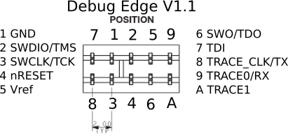
The debug edge spec support four variants, from a stripped down 4 pin version that has an edge footprint of 4mm x 4.5mm to a full 10 pin version that is 10mm x 4.5mm. The variants use a compatible pinout and simply add functionality with additional pins.
The diagram below demonstrates the pin assignment. Note that the pin numbering does NOT match the connector numbering because the connectors are renumbered by the manufacturer.
Status
This is all theoretical at this point. It is untested! We have sample boards and connectors ordered. We have not tried it in practice yet. That means we’re open to feedback! Please post an issue on one of our GitHub repos with your thoughts. Thanks!
4-pin
SWD, bring your own power
The core 4 pins feature the SWD pins used to control the target:
- SWDIO - Bidirectional data signal.
- SWCLK - Host -> Target clock signal.
It also includes shared signals:
- GND - Reference ground for the signals.
- nReset - Resets the target when set to ground.
SWD will not work with these four signals alone. It also needs a Vcc voltage reference, typically 3.3v or 5v, it is used for the high value in the signal lines. The Debug Edge host connector has a pin header to connect the Vref separately. We assume that the voltage reference is most likely to be broken out separately and is accessible, hence the subtitle, “bring your own power”.
The core 4-pin layout is designed to ground nReset when the Host and Target are flipped upside down. It is assumed that the target will high-z the remaining pins when in reset.
Host to host or target to target connections may cause trouble by grounding SWDIO.
6-pin
SWD with power and SWO
The 6-pin layout adds two additional pins:
- Vref - The high signal voltage, typically 3.3v or 5v
- SWO - Serial Wire Output, can be used for printf output
The 6-pin connector is the smallest self-contained SWD connection. It is the best footprint to use on small ARM boards.
8-pin
SWD and JTAG!
The 8-pin layout adds two additional pins, one completes the JTAG pinout and the other begins to add SWD trace support and UART output. It is the best footprint to use on small boards that require JTAG.
The JTAG pinout is:
- TMS
- TCK
- TDO
- TDI
This variant also adds UART TX, which is output from the target to the host. Make sure your host supports it.
10-pin
SWD, SWD Trace and JTAG
The 10-pin layout includes all of the bells and whistles. It is self contained and can do SWD or JTAG with a UART connection or 2-bit SWD trace.
The two additional pins are used for SWD trace data. Pin 9 can also be used for UART RX when not being used for trace.
This is the footprint to use on most hosts!
Links
Thanks
Thanks to @tachiniererin for the inspiration. Thanks to @GregDavill for suggesting the connector. Thanks to @_nitz and @tannewt for fleshing out the design and associated assets. Thanks to @k0dSE for fixing the website and suggesting UART.
Supported Boards
Host
SWD 2x5 to Debug Edge | OSH Park | GitHub